

Mohan, Lokeshwari and Ratnasingham, Sinclair R and Panidi, Julianna and Dabóczi, Mátyás and Kim, Ji-Seon and Anthopoulos, Thomas D and Briscoe, Joe and McLachlan, Martyn A and Kreouzis, Theo (2021) Determining out-of-plane hole mobility in CuSCN via the time-of-flight technique to elucidate its function in perovskite solar cells. ACS APPLIED MATERIALS & INTERFACES, 13 (32). pp. 38499-38507. ISSN 1944-8244
|
Text
am1c09750.pdf - Published Version Download (3MB) | Preview |
|
![[img]](https://real.mtak.hu/245831/7/m_am1c09750_0001.png)
|
Text (graphical abstract)
m_am1c09750_0001.png - Published Version Download (77kB) | Preview |
Abstract
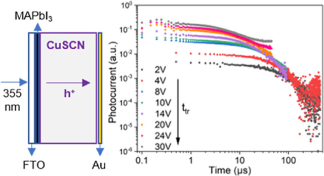
Copper(I) thiocyanate (CuSCN) is a stable, low-cost, solution-processable p-type inorganic semiconductor used in numerous optoelectronic applications. Here, for the first time, we employ the time-of-flight (ToF) technique to measure the out-of-plane hole mobility of CuSCN films, enabled by the deposition of 4 μm-thick films using aerosol-assisted chemical vapor deposition (AACVD). A hole mobility of ∼10–3 cm2/V s was measured with a weak electric field dependence of 0.005 cm/V1/2. Additionally, by measuring several 1.5 μm CuSCN films, we show that the mobility is independent of thickness. To further validate the suitability of our AACVD-prepared 1.5 μm-thick CuSCN film in device applications, we demonstrate its incorporation as a hole transport layer (HTL) in methylammonium lead iodide (MAPbI3) perovskite solar cells (PSCs). Our AACVD films result in devices with measured power conversion efficiencies of 10.4%, which compares favorably with devices prepared using spin-coated CuSCN HTLs (12.6%), despite the AACVD HTLs being an order of magnitude thicker than their spin-coated analogues. Improved reproducibility and decreased hysteresis were observed, owing to a combination of excellent film quality, high charge-carrier mobility, and favorable interface energetics. In addition to providing a fundamental insight into charge-carrier mobility in CuSCN, our work highlights the AACVD methodology as a scalable, versatile tool suitable for film deposition for use in optoelectronic devices.
| Item Type: | Article |
|---|---|
| Subjects: | T Technology / alkalmazott, műszaki tudományok > TK Electrical engineering. Electronics Nuclear engineering / elektrotechnika, elektronika, atomtechnika |
| SWORD Depositor: | MTMT SWORD |
| Depositing User: | MTMT SWORD |
| Date Deposited: | 08 Sep 2026 13:43 |
| Last Modified: | 08 Sep 2026 13:43 |
| URI: | https://real.mtak.hu/id/eprint/245831 |
Actions (login required)
 |
View Item |